Tic-Tac-Toe on a FPGA: Spring 2020
Summary
In this project, I made a Tic-Tac-Toe game using an DE1-SoC FPGA. The player uses a keyboard with a PS/2 interface to select their positions and the game is displayed on a monitor using a Video Graphics Array (VGA) interface. A high level block diagram of the system is shown in figure 1. The “Game Logic” module is responsible for alternating between the player and the AI’s turns and takes inputs from purely combinational modules which determine the AI’s move, whether the game has been won, and the player's valid move. Meanwhile, The “VGA” module is responsible for interfacing with a monitor to draw the game board. Since the area of the game board is 768x768 pixels, this module uses ROM look up tables to draw the player and AI sprites. Lastly, the "Player Input" module reads 11-bit data frames from the keyboard to determine which key has been pressed.
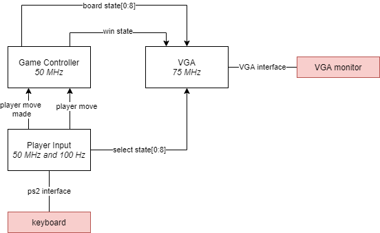
Figure 1: High-level system block diagram
Through this project I strengthened skills in Verilog and digital design. I simulated the blocks shown in figure 1 individually using ModelSim and tested them on the an FPGA. This project also taught me about mixed clock domain design since the modules had different clocks due to the PS2 and VGA interfaces.