Two Stage Op-Amp: Fall 2020
Summary
In this project, we designed a two stage op-amp to meet the requirements shown in table 1. Figure 1 illustrates the schematic of our op-amp circuit. There are four key components in this op-amp. The first component is a single ended differential amplifier that provides most of the overall amplification for the differential signal while significantly attenuating the common mode signal. A differential amplifier stage, which is the second component, outputs into a common-source amplifier that produces the remaining amplification while allowing for a large output swing. The third component is an output stage, which is a common drain amplifier and serves as a buffer. It lowers the output impedance and increases the drivability while providing unity gain. The last component is the current mirror that serves as a biasing stage and consists of transistors M1, M2, M3, M4, and M5. We added Rp and Cp to stabilize the op-amp as a part of Miller compensation.
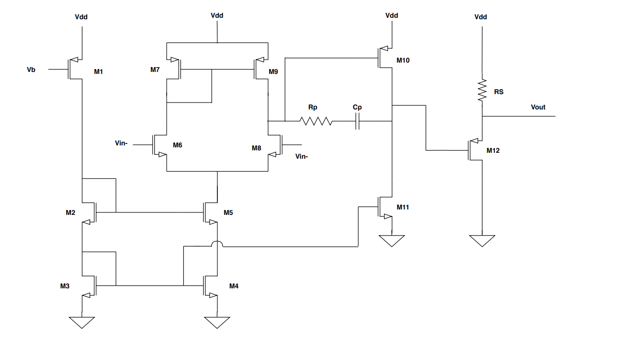
Figure 1: Circuit Diagram of Op Amp
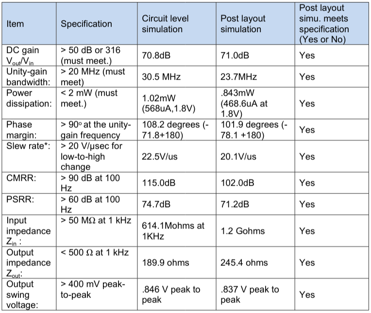
After simulating the schematic, we created the layout for the circuit as depicted in figure 2, performed parasitic extraction, and post-design simulations. Table 1 shows a comparison of the pre and post layout simulations and whether our circuit met the specifications.
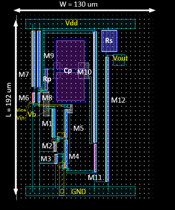
Figure 2: Layout of Op Amp
Table 1: Pre and Post Layout Performance Summary
Through this project, I gained valuable experience in designing analog circuits and simulations through Cadence Virtuoso. I also learned how to perform layout and gained skills in solving DRC and LVS errors and warnings.